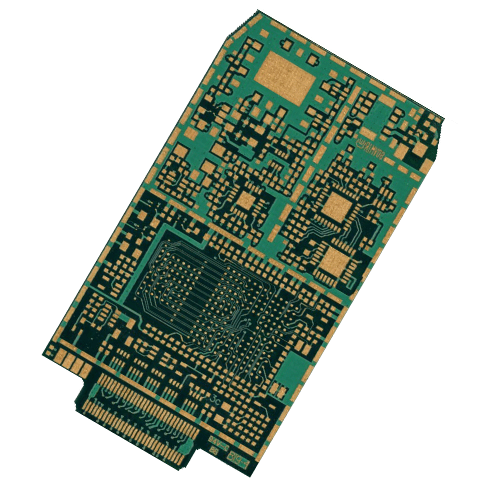
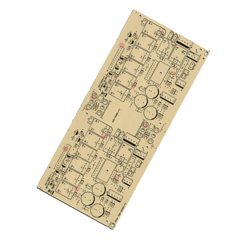
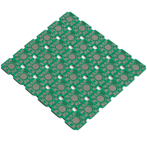
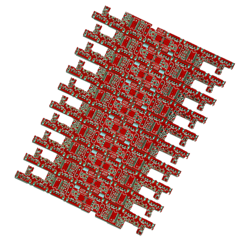
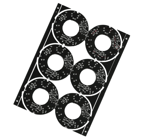
Number of Layers: four Layer Base Material: FR-4 Copper Thickness: 1OZ
Board Thickness: 1.6MM Min. Hole Size: 0.3MM Min. Line Width: 0.2MM
Min. Line Spacing: 0.2MM Surface Finishing: ENIG Color: Green
Packaging & Delivery
Packaging Detail: Inner packing: Vacuum packing / Plastic bag; Outer packing: Standard carton packing
Delivery Detail: 7-15 days
Specifications
Four layer pcb 7
Good quality, competitive price,
quick delivery and good service
We are a professional pcb manufacturer with over 20 years experence.
Sample making:6~7 days.
Mass production:7-14 business days
Our capability:
Layer: 1 to 22 layers
Material type: FR-4, CEM-1, CEM-3, High TG, FR4 Halogen Free,
Board thickness: 0.35mm to 3.0mm
Copper thickness: 0.5 OZ to 3.0 OZ
Copper thickness in hole: >25.0 um (>1mil)
The Max board size:
A,board thickness¡Ý1.2mm and Not Jack panel :605*530mm.(HASL board: 605*450mm)
B,Board thickness¡Ý1.2mm Jack panel:550*400mm
C,Board thicknss:0.5—1.2mm:400*350mm
D,Board thickness0.4mm:350*300mm
E,Single-sided board:606*530mm(board thickness>1.2mm)
F, Six layer pcb:430*430mm
G,Eight layers:430*430mm
H,more than eight layers:270*280mm
– Min. Drilled Hole Size: 10mil (0.25mm)
– Min. Line Width: 4mil (0.1mm)
– Min. Line Spacing: 4mil (0.1mm)
Surface finishing: HASL / HASL lead free, HAL, Chemical tin, Chemical Gold, Immersion Silver/Gold, OSP, Gold plating
Solder Mask Color: Green/Yellow/Black/White/Red/Blue
Tolerance
– Shape tolerance: ¡À0.15
– Hole tolerance: PTH: ¡À0.075 NPTH: ¡À0.1
PCB Packing
– Inner packing: Vacuum packing / Plastic bag
– Outer packing: Standard carton packing
Certificates: UL, ISO 9001, ISO14001; SGS,ROHS
Profiling: Punching, Routing, V-CUT


