Skip to content

CSTPCB

Shenzhen Sheng Cheng hui Circuit Science Technologies Group Co., Ltd .was founded in 1998 ,and is located in Jianshi Park, Pushang Village, Longxi Town, Boluo County, Huizhou City,Guangdong Province. There are more than 200 employees now .high-educated people accounted for 20% of the total number of workers in which senior engineers, senior technologists and other types of management personnel accounted for more than 40 people .Our factory is mainly the production of high-precision single-sided、double-side、 multi-layer rigid and flexible circuit boards. With Modern factory and advanced production equipment, We can produce 1-24 layer circuit board,and meet fastest 24-hours of delivery for double-sided PCB, 48-hour for 4 to 8 layers and 120-hour for 10 or more high-layer PCBs at the soonest. Annual PCB and FPC reach 20 thousand square meters.

Feel the History of CSTPCB

Since 1998 - Thank you for being with us for all these 25 years

Where quality matters

In recent years, The company has introduced the world advanced level of modern production ,  testing equipment and software, which can produce high-frequency,  high TG,  high CTI,  impedance control, buried and blind board ,  rigid-flexible combination , aluminum base,  HDI boards, and halogen-free  etc .In order to meet market demand, to provide customers with faster and more comprehensive support services .

In 2006, we opened our self  SMT factory in Bu Ji  dan zhu tou , undertake a variety of sophisticated electronic products processing services, as procurement different kinds of materials , SMT,  plug ,  soldering, assembly,  testing,  inspection, packing to finished one-stop EMS service.

CSTPCB, A name you can trust

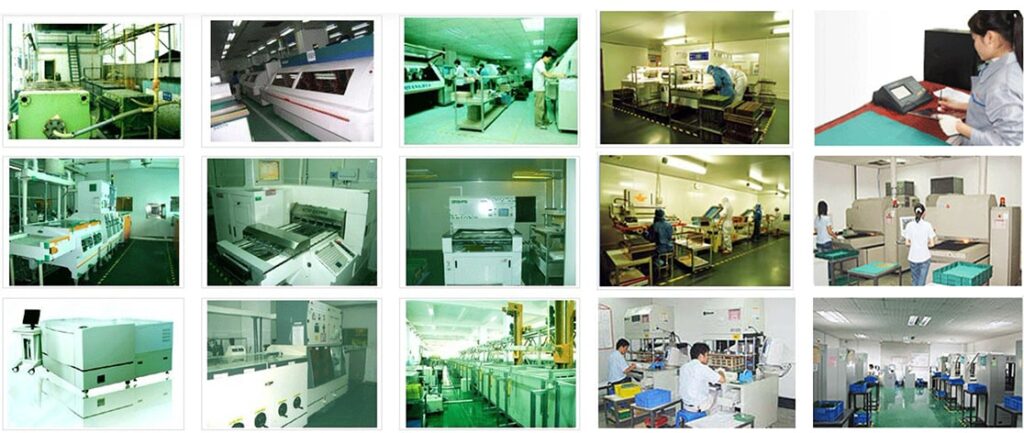
We not only own Panasonic and JUKI famous brand machine , but also introduce the latest series of foreign high-terminal and multi-function YAMAHA automatic SMT machine. There are three lines which paste 0201,  0402 package material and ultra-0.3mm pitch accuracy in QFP, BGA and other chips. Our equipment and instrument configuration is very high and more flexible like all hot air reflow oven,  dual spray-clean wave soldering DIP plug,  assembly lines,  packaging lines,  intelligent anti-static iron,  ultrasonic cleaner,  BGA rework stations, high-precision IC laser marking  and SMT leaking soldering,  joint soldering, false soldering ’s inspection AOI equipment. Advanced equipment and testing of each process can strictly control the outflow of defective products. In order to meet different customer needs, we are specially for customers to make the related membrane switch, membrane panel, touch screen and silicone rubber .

We exist for a bigger reason

Stable quality and reasonable price make our products are exported all over the world, and won wide applause from customers. Currently we have cooperated with the Panasonic, Emerson, ShunDa Computer, Flextronics and a number of Japanese, American, Taiwanese and domestic enterprises to establish a good working relationship. Since we built , the company has adhered to “provide the more excellent , fastest, best and most comprehensive service” tenet and “market-oriented, quality-centric” mode of operation, is committed to making a PCB design-PCB manufacture-SMT One-stop OEM service the most competitive companies.

Greatness Is Not an Accident

ISO 14001:2004 / ISO 9001:2008

Our Payment Methods

PAYPAL
Firstly you need to have a PAYPAL account and then come to www.paypal.com website and then send the money to :
our PAYPAL account :  nhpcbfpc@126.com

Western union
It is possible to go to post office or other banks and send money to our
pointed person (Ailing hu) by Family name Hu and First name Ailing.

美元汇款路线: INWARD REMITTANCE FOR USD
▲BENEFICIARY BANK(收款行): ZHEJIANG CHOUZHOU COMMERCIAL BANK CO.,LTD
SWIFT BIC: CZCBCN2X 银行地址(若需):NO.161 Bayi South Street Jinhua City Zhejiang Province China
▲BENEFICIARY NAME(收款人名称): Shenzhen Shengchenghui Circuit Science Technologies Co,Limited
A/C NO(帐号): NRA15901142010500000799 Company address:RM 1302 13/F CHEONG K BUILDING 84-86 DES VOEUX ROAD CENTRAL HK
▲INTERMEDIARY BANK(中间行):(Must fill in intermediary bank) BANK OF AMERICA N.A. NEW YORK (SWIFT CODE:BOFAUS3N)

RMB currency
For RMB currency ,you can send by the following account
Agricultural Bank of China
Account number : 6228480120545771715
Branch : Agricultural Bank of China ,shenzhen ‘s shangbu branch
Bank Address : First floor, World Trade Plaza ,Number 9, Fuhong Road  ,Futian district ,shenzhen ,China 
User Name: Ailing hu
Swift code : ABOCCNBJ410

Our Leadtime

Sample PCB schedule : 24-hour delivery for single and double-sided PCB, 48-hour for 4 to 8 layers and 120-hour for 10 Layers or more high-layer PCBs at the soonest.
Mass production pcb schedule : 6~8days for single and double-size pcb,8~9days for four layer pcb
12days or so for six layer or above .
Assembly schedule : 3~4day for samples and 5~6days for mass production
membrane panel and switch schedule : Six day for sample and 7~8days with mass production
silicone rubber : 10~15day building mold for sample ,and 7day for mass production

Shipment Methods

We can offer EXW, FOB, C&F,CIF and DDU shipping terms and can arrange shipment by courier, by airline or by ocean according to your requirement or we can send pointed warehouse or place if customer need to ship by themselves .

Our RFQ Rules

We can support any format for the artwork :
PCB  and FPC , BOM or sample for assembly :
Protel Dxp ,Protel 99SE,Powerpcb ,Cam350 gerber file .
Membrane Panel and Switch :
Core draw  ,CAD , PDF or only sample
Silicon Rubber Keypads :
PROE or CAD software

for pad surface ,the price is higher like as follows.
ROSIN<non rosh tin <OSP< or =Rohs tin (pb free tin)<gold.
for pcb ,0.6-0.8mm,the price will be same ;1.0-1.6,the price is same .but the thickness is 0.4 mm or below 0.4mm,the price will increase a little.
if you need 2.0mm ,the price will increase .if the thickness is above 2.0mm,we need sepcially order material.

for stencil,we can make stencil sheet without frame .we also can make stencil with frame 37*47CM or 42*52CM or others. stencil sheet is cheaper than with frame stencil.
for complex IC ,small o402 part,or BGA,they are better to open laser stencil .but price will be increasing some.
if the pcb part is near board edage ,when we make pcb ,we need to add board edage.
sometime, big SMT part,we use machine not by hand which do SMT ,and we also add some gap .so that there have enough room and make array on the panel.
so the board edage and gap will also cause price increasing because we need to use extra more material and enlarge pcb area.
FLUX =OSP
ENIG=immersion gold
HASL =Pasted non rosh tin on the pad surface
HASL PB FREE=pasted rosh tin on the pad surface